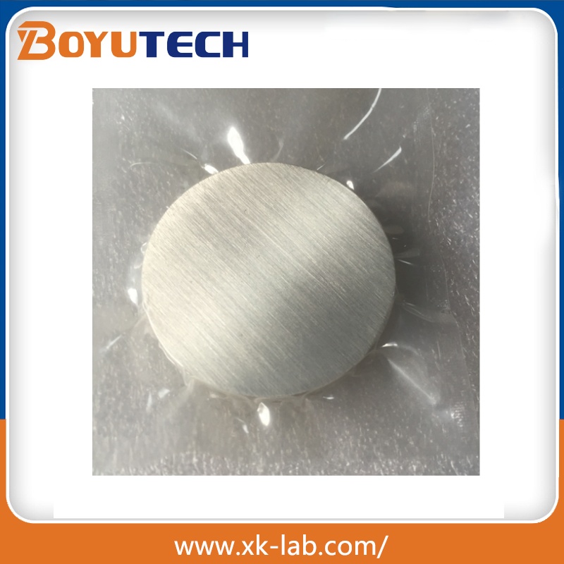
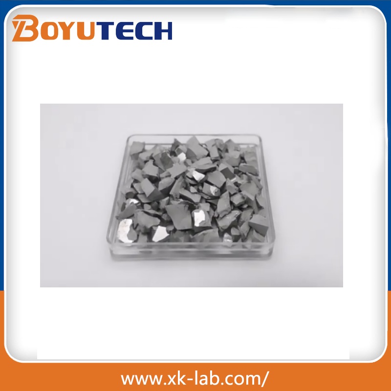
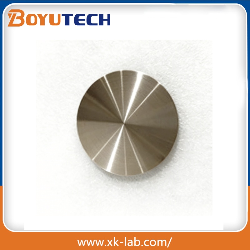
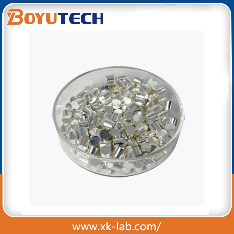
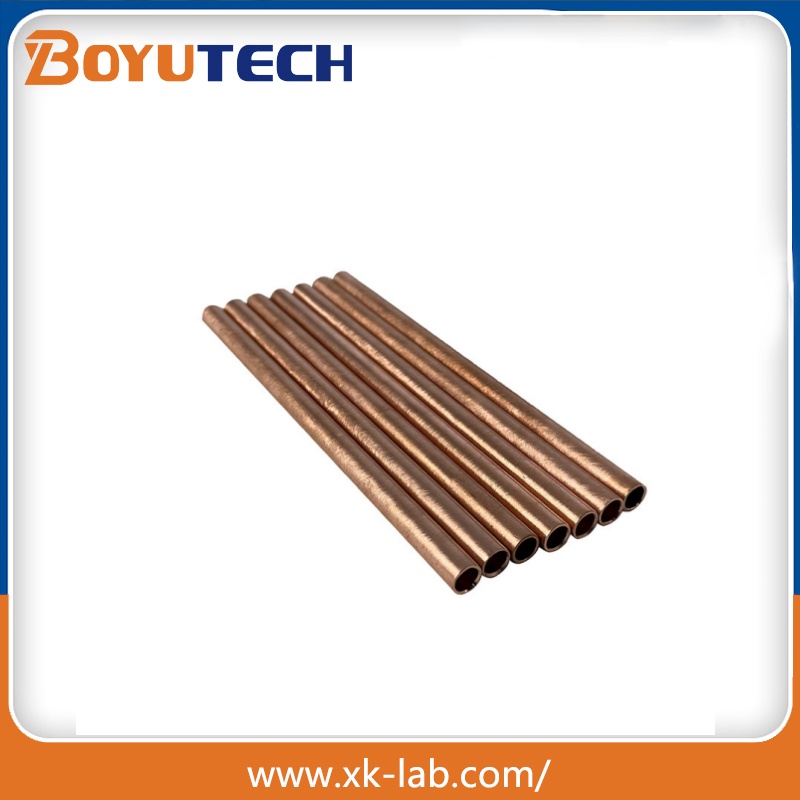
全部产品
产品分类背景图

Copper (Cu) Sputtering Target


材料类型 Cu Target
元素符号 Cu
原子量 3N5,4N,4N5,5N,6N
原子序数 As request
颜色/外形 Planar,Disc,Rotary etc
热导率 1-3week W/m.K
熔点 Support Customize (°C)
沸点 Support (°C)
热膨胀系数 Semiconductors, display panels, optics, solar energy, and functional coatings /K
产品简介

Copper (Cu) Sputtering Target Description:


Copper (Cu) sputtering targets are high-performance conductive materials, widely used for depositing high-purity, high-conductivity thin films in various industrial and electronic fields. With excellent electrical conductivity, thermal conductivity, ductility and good film adhesion, copper sputtering targets are ideal for preparing conductive layers, interconnection lines and functional coatings, and are core materials in semiconductor, optoelectronic, and decorative coating applications.
Purity Specification (Core Purity Information):
Purity Grade
Application Characteristics
3N5 (99.95%)
The most commonly used conventional purity grade, suitable for most industrial and electronic applications, such as general conductive films, decorative coatings, and common electronic component interconnection layers. It has excellent cost-effectiveness and stable performance, meeting the basic requirements of most sputtering scenarios.
4N (99.99%)
High-purity grade, suitable for mid-to-high-end electronic and optoelectronic applications, such as semiconductor auxiliary conductive layers, optoelectronic device electrode layers. It effectively reduces impurity interference and ensures the stability of film performance.
4N5 (99.995%)
High-purity grade for precision electronic applications, such as high-end semiconductor wafers, precision sensors and other products that have strict requirements on impurity content, ensuring the stability and reliability of core components.
5N (99.999%)
Ultra-high purity grade, mainly used in cutting-edge scientific research, high-precision electronic devices and special functional film preparation, with extremely low impurity content and excellent film forming quality.
6N (99.9999%)
Top-level ultra-high purity grade, used in high-end semiconductor chips, advanced optoelectronic devices and key scientific research fields, which can maximize the reduction of impurity impact and ensure the ultimate performance of products.
Semiconductor & Microelectronics
Widely used as conductive interconnection lines, electrode layers and diffusion barrier auxiliary layers in integrated circuits, wafers and electronic packaging, effectively ensuring stable signal transmission and improving device conductivity.
Optoelectronic & Display Devices
Applied to deposit conductive thin films for displays, solar cells, and optoelectronic sensors, leveraging copper’s excellent electrical and thermal conductivity to enhance device energy conversion efficiency and signal stability.
Decorative & Functional Coatings
Suitable for preparing decorative copper coatings on hardware, architectural parts and consumer electronics, with a bright surface finish and good corrosion resistance, while also serving as a functional conductive layer in various devices.
Industrial & Other Applications
Used in magnetic storage devices, electromagnetic shielding coatings and industrial conductive components, meeting the high-conductivity and high-reliability requirements of different industrial scenarios.

Copper sputtering targets with different purity grades are compatible with DC and RF magnetron sputtering systems, ensuring stable deposition, uniform film thickness and high film purity, which can fully meet the application needs of different precision levels in various fields.

Related Sputtering Targets
CuAl Sputtering Target
CuB  Sputtering Target
CuCr Sputtering Target
CuNi Sputtering Target


咨询我们